
Augmented Silkscreen
Designing AR Interactions for Debugging Printed Circuit Boards
By 2030, the number of smart devices in the world is projected to reach 50 billion. The proliferation of these devices can largely be attributed to the increasingly integrated nature of electronics and silicon, as per Moore’s law. Just as the number of transistors in an integrated circuit (IC) have increased exponentially, so too have printed circuit boards (PCBs) become increasingly dense with electronic components.
These denser and more complex PCBs pose greater challenges for electrical engineers during the debugging process. However, the tools used to support these engineers in debugging faulty PCBs during design and development remain largely unchanged. During the process of debugging a new PCB design, electrical engineers must constantly move between circuit diagrams, board layout diagrams, and the physical circuit board itself in order to validate their design or understand the nature of a design failure.
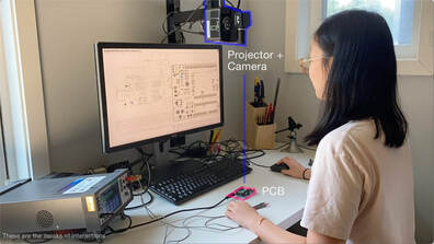
To reduce this overhead, we conduct a series of interviews with electrical engineers to understand their workflows, around which we design a set of AR interaction techniques, we call Augmented Silkscreen, to streamline identification, localization, annotation, and measurement tasks. We then run a set of remote user studies with illustrative video sketches and simulated PCB tasks to compare our interactions with current practices, finding that our techniques reduce completion times. Based on these quantitative results, as well as qualitative feedback from our participants, we offer design recommendations for the implementation of these interactions on a future, deployable AR system.
These denser and more complex PCBs pose greater challenges for electrical engineers during the debugging process. However, the tools used to support these engineers in debugging faulty PCBs during design and development remain largely unchanged. During the process of debugging a new PCB design, electrical engineers must constantly move between circuit diagrams, board layout diagrams, and the physical circuit board itself in order to validate their design or understand the nature of a design failure.
To reduce this overhead, we conduct a series of interviews with electrical engineers to understand their workflows, around which we design a set of AR interaction techniques, we call Augmented Silkscreen, to streamline identification, localization, annotation, and measurement tasks. We then run a set of remote user studies with illustrative video sketches and simulated PCB tasks to compare our interactions with current practices, finding that our techniques reduce completion times. Based on these quantitative results, as well as qualitative feedback from our participants, we offer design recommendations for the implementation of these interactions on a future, deployable AR system.
|
Citation
Ishan Chatterjee, Olga Khvan, Tadeusz Pforte, Richard Li, and Shwetak Patel. 2021. Augmented Silkscreen: Designing AR Interactions for Debugging Printed Circuit Boards. In Designing Interactive Systems Conference 2021 (DIS '21). Association for Computing Machinery, New York, NY, USA, 220–233. DOI:https://doi.org/10.1145/3461778.3462091 | ||
|
Short Video:
|
Conference Presentation:
|
|
|
|
© Ishan Chatterjee 2023
